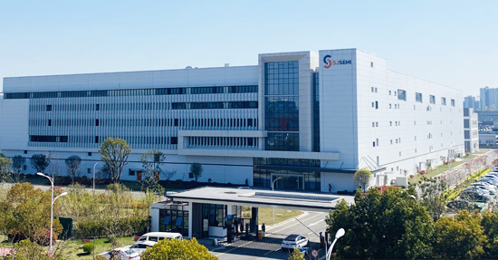
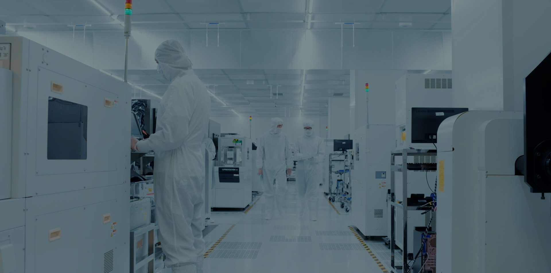
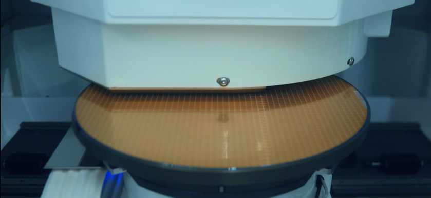
SJSemi is the first Middle-End-Of-Line (MEOL) pure play foundry equipped with Front-End-Of-Line (FEOL) manufacturing and quality system, serving global customers.

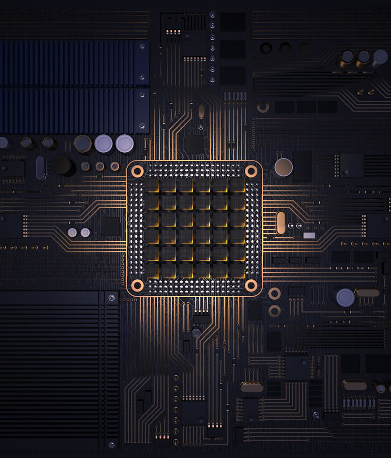
SJSemi devotes to offer first-class Middle-End-Of-Line (MEOL) manufacturing and testing services and develops to provide the advanced 3D Multi-Die Integration technology and solutions.

SJSemi is the first Middle-End-Of-Line (MEOL) pure play foundry equipped with Front-End-Of-Line (FEOL) manufacturing and quality system, serving global customers.

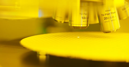
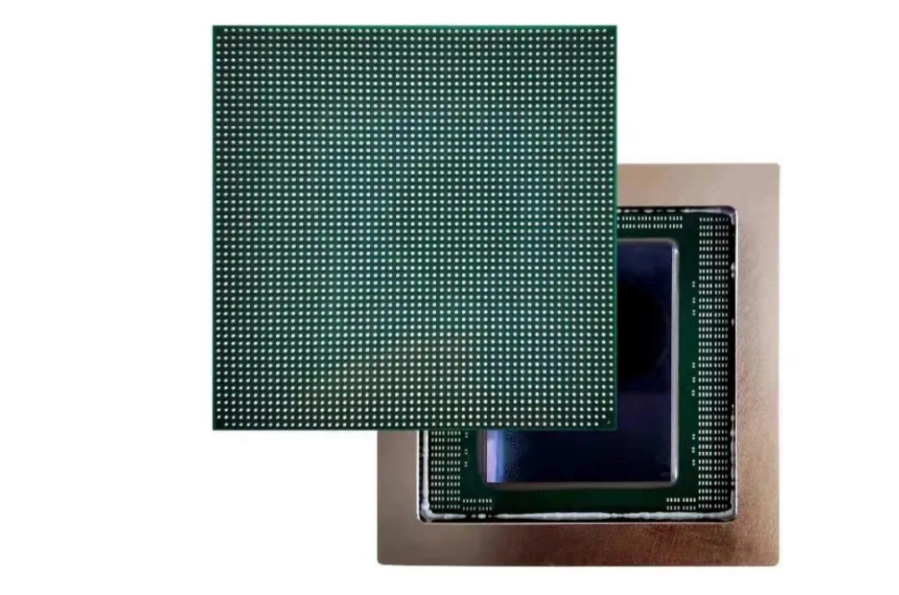
Bumping is a wafer level advanced packaging technology. The bumps are typically formed upon under bump metallization (UBM) which is electroplated on the die pads openings.
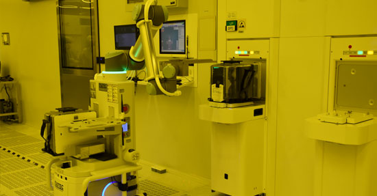
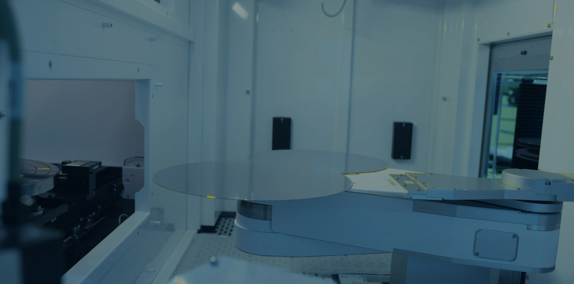
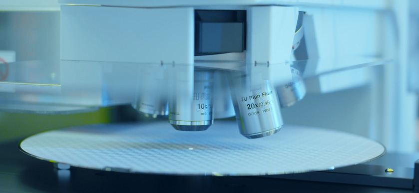
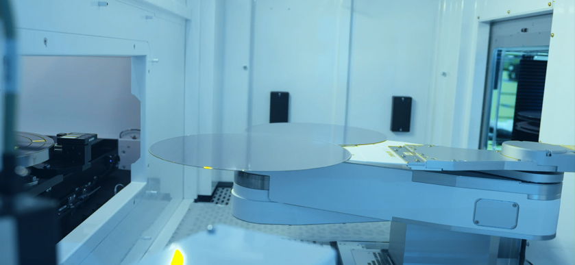
CP (Chip Probing) is to test the electrical and functional performance of the chips on wafer level by using Automatic Test Equipment(ATE) and probe cards.
SJSemi’s WLCSP solution providing the best service to global top chip design houses and end product customers, can meet different product application and technologies.
SJSemi is the first Middle-End-Of-Line (MEOL) pure play foundry equipped with Front-End-Of-Line (FEOL) manufacturing and quality system, serving global customers.
SJSemi devotes to offer first-class Middle-End-Of-Line (MEOL) manufacturing and testing services and develops to provide the advanced 3D Multi-Die Integration technology and solutions.