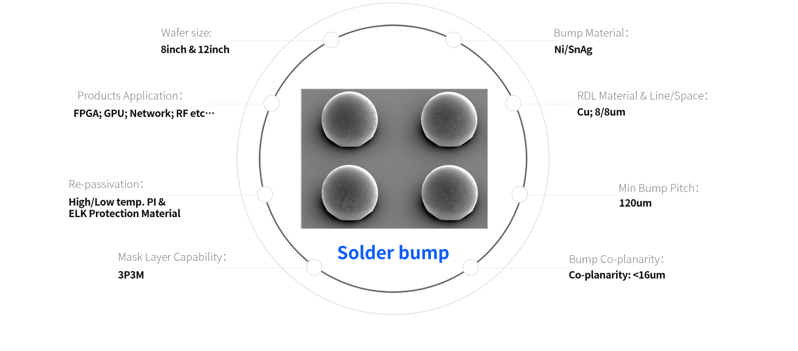
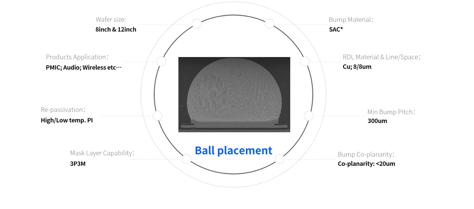
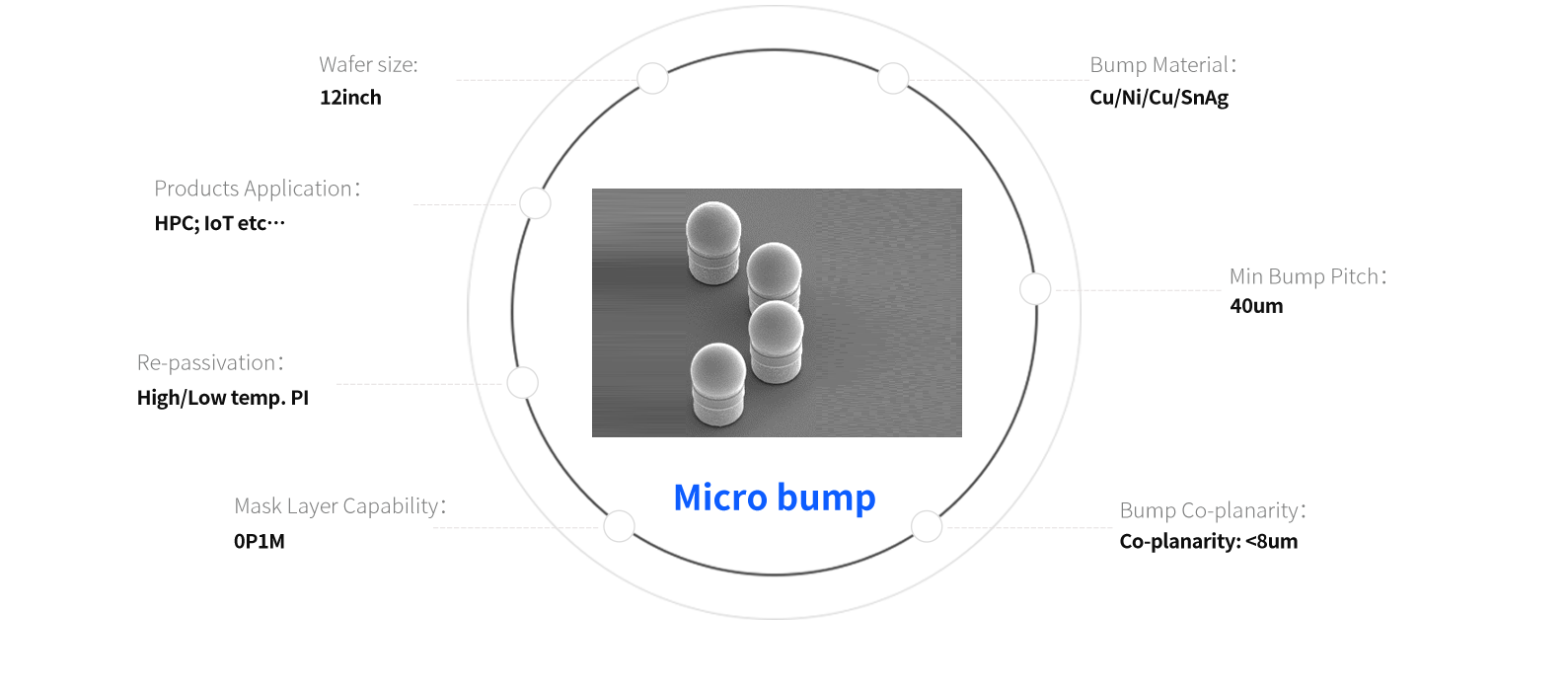
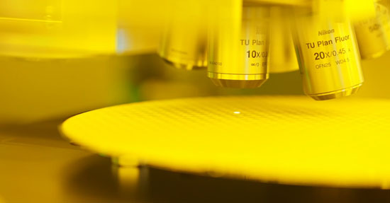
Bumping is a wafer level advanced packaging technology. The bumps are typically formed upon under bump metallization (UBM) which is electroplated on the die pads openings. The bumps can be of different materials, depending on the applications. Lead free bump (SnAg) are is generic and copper pillar bump can offer the advantage of much higher I/O density.
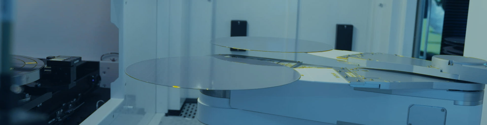

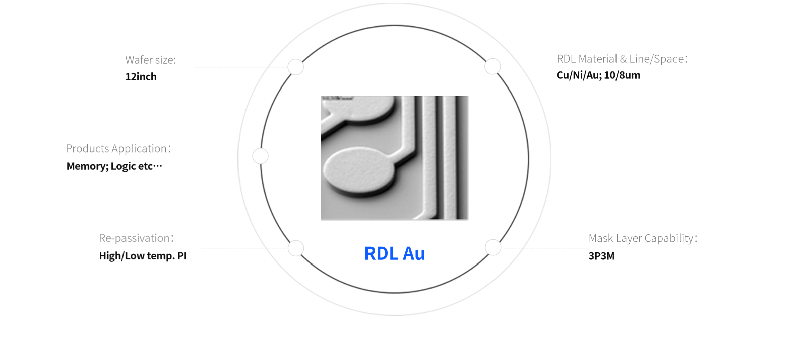
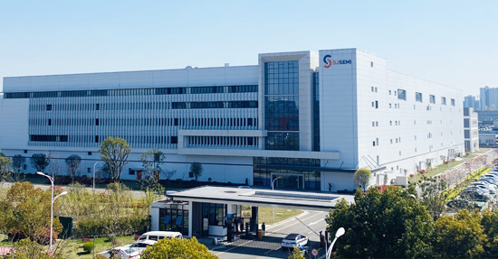
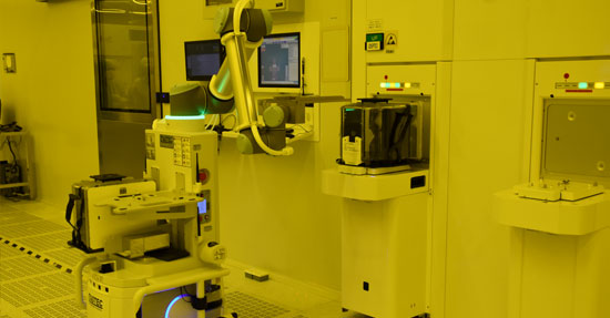
With variety of middle-end bumping technologies, experienced professional engineering team and highly automated production system, SJSemi is committed to provide high quality 200mm and 300mm wafer bumping services.