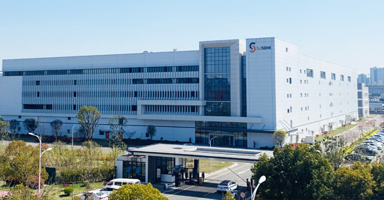
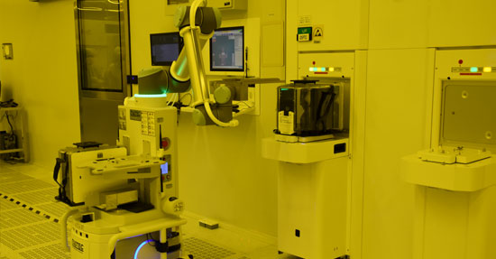
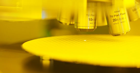
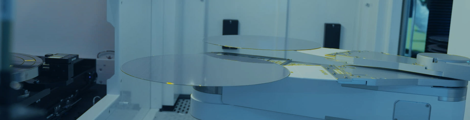
As performance, form factor, power consumption and cost become more demanding for mobile and portable devices, WLCSP (Wafer Level Chip Scale Packaging) gained more popularity by leveraging wafer process to achieve higher interconnect density, better performance and power consumption with more compact form factor , which is a good fit for mobile and wearable applications,SJSemi is one of the pioneers of WLCSP in China .We provide 200/300mm FI/FO packaging, multiple layer/double side RDL, wafer thinning and saw with ELK laser grooving , frame form or tape/reel shipping along with CP testing for one-stop WLCSP service.

SJSemi’s WLCSP solution providing the best service to global top chip design houses and end product customers, can meet different product application and technologies. To serve the rapid growing market of 12” WLCSP with Low-K, we offer total solution packed with laser grooving technology as well as ELK crack defect QC control for wafer saw.WLCSP with nodes above 28nm are in mass production, and 22nm is completing its qualification. DBG(Dicing Before Grinding) technology is offered for ultra-thin die solution as well . SJSemi has business connections for with all leading foundry worldwide, offers full turnkey one-stop solution from Bumping/RDL, CP, die singulation and packaging shipment in frame or tape/reel.